The Basics of Flexible Circuit Board Design
Most every device and electronic piece of equipment is outfitted with a printed circuit board (PCB), including smartphones, TVs, appliances, and more. You know the composite. The boards are laminated structures of conductive insulated layers that provide two different functions: hosting electronic components in designated areas on the outer layers and providing reliable electrical connections between the component terminals and conductive pads.
Those electronic components—resistors, capacitors, microcontrollers, interfaces, etc.—are electronically connected via traces, planes, and other features using a chemical etching process that deposits copper layers laminated onto sheets of a non-conductive substrate.
PCBs were developed in the early 20thcentury, and while they have continued to evolve with the onset of new technologies, their fundamental design has remained essentially unchanged—a rigid board populated with electronic components.
The advancement and widespread adoption of technology in PCBs has paralleled the rapid advances in semiconductor packaging technology, enabling industry professionals to invest in smaller and more efficient electronics. It’s led to the development of wearable technologies, such as AR/VR glasses, smartwatches, and even interactive clothing.
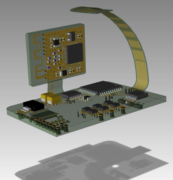
It’s also ushered in the era of formfitting medical devices capable of monitoring the wearer's health via direct contact with the skin and smartphones using folding displays, among other technologies. To realize those devices, a new type of PCB needed to be developed, one that could stretch and warp beyond right angles. Engineers rose to the challenge to create flexible circuit boards using various techniques and materials, including polyimides, transparent polyester, and more (Fig. 1).
Manufacturers have adopted two types of malleable boards for today's devices: flexible and rigid-flex PCBs. Flexible PCBs, or flexible circuit boards (FCBs), function similarly to their rigid counterparts, wherein the electronics are placed on a flexible substrate rather than a rigid platform. This makes it possible to form the electronics in different shapes and configurations instead of a planar surface. Based on the layer and configuration, these can be broken down to the two most common types mentioned earlier.
Rigid-flex PCBs are hybrids, boards that are both rigid and flexible to accommodate an arrangement of SMDs (surface-mounted devices, aka electronics) and connectors. In this configuration, the SMDs are mounted on a flexible substrate while the connectors reside on a rigid surface to maintain a stable connection and mitigate any damage from repeated use. The rigid-flex configuration also allows for increased capacity of SMDs because the connection terminations are placed on the rigid surface.
High-density interconnect (HDI) PCBs offer a higher wiring density over their rigid counterparts and provide much finer lines and spaces, smaller vias and capture pads, and higher connection pad density. These PCBs are beneficial when applied with flexible substrates, as they can take advantage of thinner layers or, in some cases, eliminate the need for many layers in the PCB design.
Classification of FCBs can be broken down by the number of layers. For example, single-layer boards are created using a single polyimide substrate and thin copper layer, which can be accessed from one side of the board. There are also single-sided FCBs with dual access, double-sided FCBs that have electrically conductive copper on both sides of the substrate, and multi-layered FCBs with multi- and single-sided access features.

Many questions come into play when designing a flexible PCB (Fig. 2), with the most important being how many times it will flex and to what extent it will flex. The number of times it can bend determines whether the board will be static or dynamic.
A static board is considered bend-to-install and will flex less than 100 times in its lifetime. A dynamic board's design needs to be more robust, as flexing will be done regularly and might need to withstand tens of thousands of bends depending on the application. Of course, the bend radius—the minimum amount of curvature for the flex area—comes into play, too, and must be appropriately identified early in the design. This ensures that the design can withstand the necessary amount of bends without damaging the copper.
Solder masks and other materials that cover the conductive layers of the FCBs also must be considered during the design phase, as well as a stiffener, which is used to support different parts of the circuit and can be used on both sides of the board. It's important to note that the amount of stiffener applied will add to the rigidity of the design, lessening the flex in some or all areas.
As with traditional PCBs, FCBs have a layered design, so the material used also must be considered during the design phase. For example, a film layer supplies the conductor carrier and acts as an insulator in the circuit, but it must be flexible as well. Polyimide and PET (polyester) work well as insulators and are typically used for these kinds of substrates. PEN (polyethylene phthalate), PTFE and Aramid are utilized, too.
Polyimide flex cores also work in FCB designs. They’re cladded with either electrodeposited or rolled annealed copper, which is super thin and suitable for dynamic and static applications.
FCBs take advantage of two types of materials: adhesive-based, where the copper is bonded to the polyimide with acrylic adhesive; and adhesive-less, which casts the copper directly onto the polyimide substrate. Of course, adhesive materials have their drawbacks, including causing cracks to form when subjected to heat. They also make the copper laminate thicker and tend to absorb moisture, preventing them from being utilized in some environments.
This is where adhesive-less materials come into play. They can handle harsh environments and provide other benefits, including reduced flex thickness, improved flexibility, and better temperature ratings.
PCB stacks are the arrangement of layers of copper and insulators that make up a PCB before designing the final layout of the board (Fig. 3). While a stack-up level allows you to assemble multiple electronic circuits on a single board through its various layers, the structure of the PCB stack-up design provides many other advantages, including mitigating external noise, improve electromagnetic compatibility, and reducing manufacturing costs. Using multiple layers increases the board's ability to distribute energy, reduces cross-interference, eliminates electromagnetic interference, and supports high-speed signals.
As with traditional PCBs, FCBs can be designed using one or more layers and denote the number of copper traces, adhesive, laminates and polyimide materials. These numbers rise depending on the number of layers. For example, a four-layer circuit will have four copper traces, four layers of adhesives (or non-adhesives), laminates, and corresponding substrate materials. Many manufacturers will place the flex material at the center of the stack-up to maintain flexibility and mitigate any damage during operation.
When deciding the number of layers, it's essential to consider several factors before committing to a design, including the number of circuit signals that need to be routed, operating frequencies, whether it needs additional shielding and other metrics. These will help to denote the exact number of needed layers and ensure the FCB functions as intended.
Flexible printed circuit boards will continue to evolve as new technologies become available. Imagine being able to clean a medical monitoring device in the laundry or wearing a biometric patch while diving in the ocean without worrying about corrosion.
Already, devices can grab data from within the human body that rely on flexible electronics, so it will be interesting to see where this technology will be implemented. It's also important to note that this is simply a basic introduction to flexible PCB design, providing an overview of the materials and processes used to create them.
}})
George Washington
Lorem ipsum dolor sit amet, consectetur adipisicing elit. Ducimus itaque, autem necessitatibus voluptate quod mollitia delectus aut, sunt placeat nam vero culpa sapiente consectetur similique, inventore eos fugit cupiditate numquam!